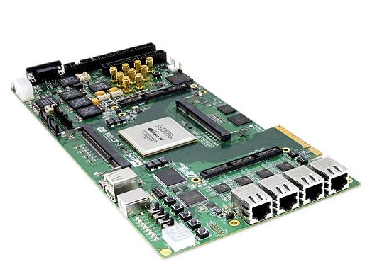
Terasic Altera DE4 开发和教育模块
制造商: Terasic Model: DE4 - 联系
1. FPGA Devices
-Stratix IV GX EP4SGX230
+ 228,000 logic elements (LEs)
+17,133K total memory Kbits
+1,288 18x18-bit multipliers blocks
+2 PCI Express hard IP blocks
+744 user I/O
+8 phase locked loops (PLLs)
-Stratix IV GX EP4SGX530
+531,200 logic elements (LEs)
+27,376K total memory Kbits
+1,024 18x18-bit multipliers blocks
+4 PCI Express hard IP Blocks
+744 user I/Os
+8 phase locked loops (PLLs)
2. FPGA Configuration
+JTAG and Fast Passive Parallel (FPP) configuration
+On-board USB Blaster
3. Memory Devices
+64 MB Flash with a 16-bit data bus
+2 MB ZBT SSRAM
+I2C EEPROM
4. Kit Contents
+DE4 Development Board
+Power supply (250W)
+Altera Complete Design Suite DVD
+DE4 Development Kit CD-ROM
+AC power cord (Type B North American plug)
+Fan (installed)
+Type A-B USB cable
+HSMC debug board
+USB to SD Card adapter
+2G SD Card
+Screw and copper pillar package
+PCIe bracket
+HSMC loopback adapter x2
+DDR2-800 1GB SO-DIMM module
+THCB-HMF2 (HSMC Height Extension Male to Female card) x2
+DE4 power cable
+PCIe power cable
+Ethernet Cat 5e cable SATA cable x2
+DE4 Quick Start Guide
The DE4 Development Board provides the ideal hardware platform for system designs that demand high-performance, serial connectivity, and advanced memory interfacing. Developed specifically to address the rapidly evolving requirements in many end markets for greater bandwidth, improved jitter performance, and lower power consumption. The DE4 is powered by the Stratix® IV GX device and supported by industry-standard peripherals, connectors and interfaces that offer a rich set of features that is suitable for a wide range of compute-intensive applications. The evaluation of transceiver performance for jitter, protocol compliance, and equalization on the DE4, exceeded the Stratix IV GX performance standard with transceivers operating at 10 Gbps on SATA and HSMC interfaces!
The advantages of the Stratix® IV GX FPGA platform with embedded transceivers has allowed the DE4 to fully compliant with version 2.0 of the PCI Express standard in addition to serial ATA (SATA) interfaces making it possible to leverage the integration option for storage applications. The DE4 delivers fully tested and supported connectivity targeted reference design that integrates built-in blocks for PCI Express, SATA transceivers, and Gigabit Ethernet protocol. Situated on the DE4 also includes two DDR2 SO-DIMM socket supporting maximum capacity of 8-Gbyte of volatile memory for user applications which are capable running at 400 MHz clock rate.
The DE4 is supported by multiple targeted reference designs and two High-Speed Mezzanine Card (HSMC) connectors that allow scaling and customization with mezzanine daughter cards. For large-scale ASIC prototype development, it can be established by a cable connecting to multiple DE4/FPGA boards through the HSMC connectors.
- 质量承诺
- 正品保修
- 送货到家
- 交易简单化
