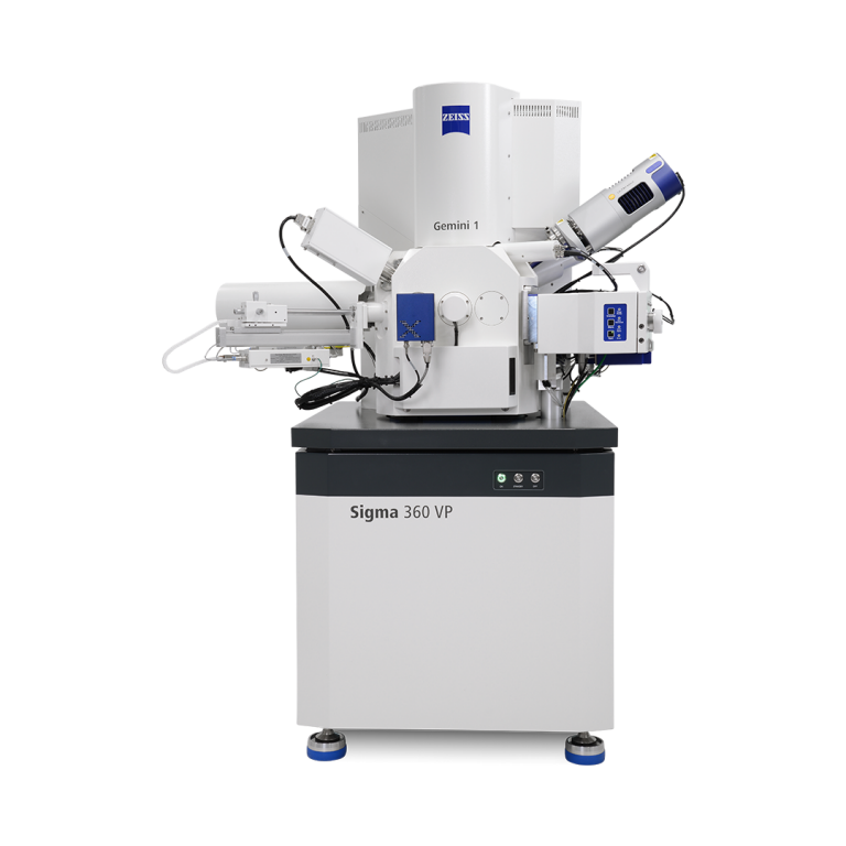
ZEISS Sigma 300 Electron Microscopy
Manufacturer: ZEISS Model: Sigma 300 Origin: Germany - Contact
Call for the best price
Hanoi city: (024) 35.381.269
Danang city: (023) 63.747.711
Bac Ninh city: (0222)730.39.68
HCM city: (028) 38.119.636
Electron Source: Schottky Thermal Field Emitter Schottky Thermal Field Emitter
Resolution* at 30 kV (STEM): 1.0 nm
Resolution* at 15 kV: 0.9 nm
Resolution* at 1 kV: 1.3 nm
Resolution at 500 V: 1.9 nm
Resolution* at 30 kV: (VP Mode) 2.0 nm
Accelerating Voltage: 0.02 – 30 kV
Magnification: 12× – 1,000,000×
Field of View: 4.6 mm
Probe Current 3 pA - 20 nA (100 nA optional)
Image Framestore: 32 k × 24 k pixels
Type of Diode: Silicon based diode for direct detection of backscattered electrons, one segment
Image Polarity: Configurable. Default: “TEM” like contrast
Optimum Working Distance: 4 – 6 mm
Energy Range: < = 7 keV
Optimum Primary Beam Current: 50 pA – 1nA
Mechanical Module: Highly stable mechanical module with acoustic dampening cover
Easy Servicability: Diode exchange is plug & play
Protection:
Protective cover to avoid charging and damage to the diode.
Integrated protection during plasma cleaning of sample/chamber.
Lifetime: Expected lifespan of detector diode: 2 years under average usage conditions
System Integration:
Collision control with ZEISS hardware implemented.
Acceleration voltage limited to <7 kV.
EO table correction is applied.
User Interface: Default settings optimized for ease of use.
Insertion and Retraction: Pneumatic
- Quality Engagement
- Easy change and return
- Delivery Avaliable
- Favorable payment