Raman spectrometer
When material identification has to be fast, non-destructive, and reliable, Raman spectrometers become an important tool in both laboratory analysis and industrial inspection. By reading the characteristic vibrational signature of a sample, Raman measurement helps users verify composition, check material consistency, and support decisions without cutting or contaminating the product.
This category brings together handheld, compact, and in-situ Raman systems suited to different workflows. Whether the task involves incoming material verification, routine QA in regulated environments, field inspection, or process observation inside liquids and slurries, the available range covers practical needs from mobility to deeper analytical control.
Why Raman spectroscopy is widely used in modern testing workflows
Raman spectroscopy is valued because it can analyze many materials with minimal sample preparation. A laser is directed onto the sample, and the returned spectral information reflects molecular or crystal vibrations that are characteristic of the substance being tested. In practice, this makes Raman useful for identifying unknowns, checking purity, comparing batches, and monitoring structural changes.
Another advantage is its role as a non-destructive analysis method. In many workflows, preserving the sample is essential, especially when working with high-value materials, finished goods, tablets, packaged substances, or research samples. For organizations building a broader test setup, it can also be useful to review related laboratory equipment options that support sample handling and routine lab operations.
Handheld, compact, and in-situ systems for different operating needs
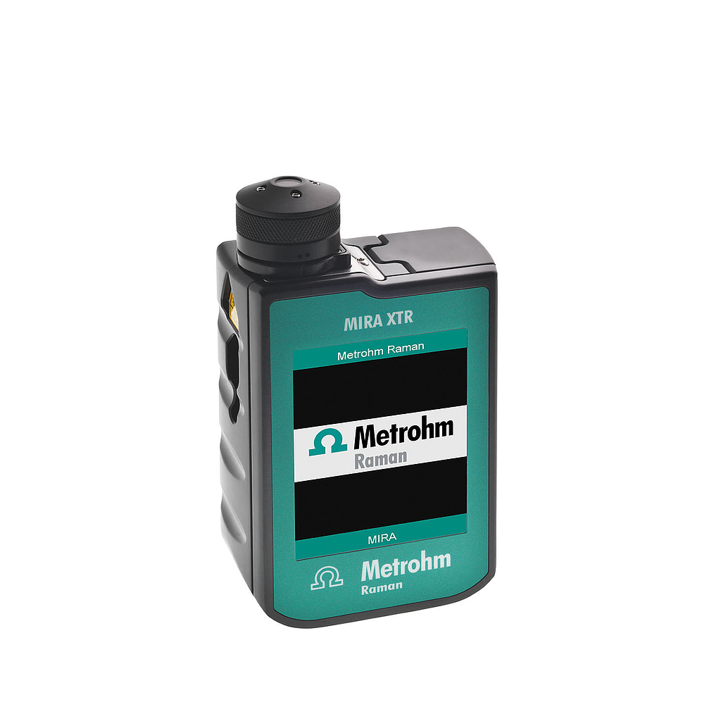
Not every Raman application requires the same instrument format. Handheld systems are often chosen for fast identification at the point of use, especially when operators need to move between storage, production, or inspection areas. A model such as the Anton Paar Cora 100 is designed for portable work, while Metrohm handheld devices such as the NanoRam-1064, TacticID Mobile, and TacticID N Plus illustrate how Raman can be deployed directly in the field.
Compact direct-measurement systems fit applications where users want bench-level convenience with simplified operation. Examples in this category include the Anton Paar Cora 5001 Direct and Cora 5001 Direct Pharma, both positioned for routine analysis with a compact footprint. For more flexible sampling away from the main instrument, fiber-based configurations such as the Anton Paar Cora 5001 Fiber Standard or Cora 5001 Fiber Process Monitoring allow measurements to be taken at the sample location rather than only inside the device housing.
Typical applications across laboratories and production environments
Raman spectrometers are commonly used for material identification, raw material verification, and quality control. In research and industrial settings, they can help characterize solids, powders, liquids, and selected packaged materials by comparing measured spectra against reference data or expected signatures. This supports faster release decisions and more consistent product evaluation.
They are also relevant when users need to observe structural or compositional changes during production. Fiber-probe systems such as the Anton Paar Cora 5001 Fiber Process Monitoring are especially suitable where measurement must be performed inside process media, including liquids or slurries. In regulated workflows, models such as the Cora 5001 Fiber Pharma and Cora 5001 Direct Pharma add context for users who need better traceability, guided operation, and secure data handling.
What to consider when selecting a Raman spectrometer
The right choice depends first on the sampling environment. If testing happens in warehouses, receiving areas, or multiple inspection points, a portable instrument with battery operation and straightforward export options may be more practical. If the work is done in a controlled lab and involves method development, library management, or repeated daily analysis, a compact or fiber-based platform may provide a better fit.
It is also important to consider laser wavelength, spectral range, safety approach, connectivity, and how the data will be used. Some users prioritize touchscreen operation, Wi-Fi or USB transfer, and onboard storage for routine workflows. Others focus more on compliance support, user permissions, and compatibility with established procedures. If your workflow includes broader brand standardization, it may be helpful to explore the available range from Anton Paar or compare handheld options from Metrohm.
Examples from the product range
Within portable measurement, the Anton Paar Cora 100 offers a compact handheld format with 785 nm excitation and a spectral range suited to rapid spot checks and field use. Metrohm also contributes several handheld options, including the NanoRam-1064 and TacticID series, which are relevant where mobility, touchscreen operation, and wireless connectivity are part of the working requirement.
For users who need broader workflow flexibility, the Anton Paar Cora 5001 family covers several practical scenarios. The Fiber Standard version supports remote probe-based measurement, the Fiber Pharma version addresses regulated analytical routines, and the Fiber Process Monitoring version is aimed at real-time insight in process environments. The Direct and Direct Pharma models are more suitable when samples can be measured directly on a compact instrument with tailored accessories for different sample forms.
Data handling, traceability, and routine usability
Beyond optical performance, day-to-day usability has a direct effect on how valuable a Raman system becomes. Features such as touch interfaces, USB or Ethernet connectivity, export to common file formats, and onboard storage help simplify review and reporting. These details matter in busy labs where operators need results that are easy to move into existing documentation or quality systems.
For some organizations, traceability and compliance are just as important as the spectrum itself. In those cases, workflow features such as user roles, password-protected access, versioned methods, and controlled reference libraries can reduce risk in routine operations. This is especially relevant in pharmaceutical or tightly managed industrial environments where auditability and repeatability are part of the purchasing criteria.
How Raman fits into a broader lab ecosystem
A Raman spectrometer rarely works in isolation. Sample presentation, transport, storage, and operator safety all influence the effectiveness of the measurement process. Depending on the application, users may also need supporting items such as carts and trolleys for instrument movement or handling accessories for organized workflow inside the lab.
Because this category covers both mobile and benchtop-oriented instruments, it can support different stages of analytical work, from quick screening to more structured routine testing. Choosing the right platform is usually less about finding one universal device and more about matching the instrument format to the real operating environment, sample type, and data expectations.
Choosing with application needs in mind
The strongest buying decisions usually start with the actual task: identify unknown materials quickly, verify incoming goods, support regulated release, or observe a process in real time. Once that use case is clear, it becomes easier to narrow the choice between handheld systems, direct compact instruments, and fiber-based Raman solutions.
This Raman spectrometer category is built to support that comparison process in a practical way. By reviewing instrument format, measurement approach, data workflow, and application fit, buyers can move toward a system that supports both current testing needs and future expansion without overcomplicating routine operation.
-
-
-
-
-
-
-
-
-
-
-
-
-
-
-
-
-
-
-
-
-
-
-
-